- 您现在的位置:买卖IC网 > Sheet目录3818 > PIC18F4620-I/ML (Microchip Technology)IC MCU FLASH 32KX16 44QFN
PIC17C4X
DS30412C-page 162
1996 Microchip Technology Inc.
Applicable Devices 42 R42 42A 43 R43 44
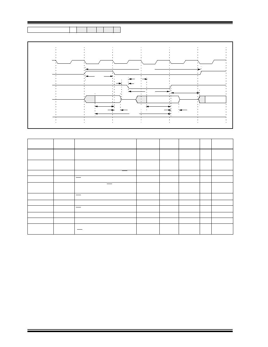
FIGURE 17-12: MEMORY INTERFACE READ TIMING
TABLE 17-12: MEMORY INTERFACE READ REQUIREMENTS
Parameter
No.
Sym
Characteristic
Min
Typ
Max
Units Conditions
150
TadV2alL
AD<15:0> (address) valid to ALE
↓
(address setup time)
0.25Tcy - 30
—
ns
151
TalL2adI
ALE
↓ to address out invalid
(address hold time)
5*
—
ns
160
TadZ2oeL
AD<15:0> high impedance to OE
↓
0*
—
ns
161
ToeH2adD
OE
↑ to AD<15:0> driven
0.25Tcy - 15
—
ns
162
TadV2oeH
Data in valid before OE
↑
(data setup time)
35
—
ns
163
ToeH2adI
OE
↑to data in invalid (data hold time)
0
—
ns
164
TalH
ALE pulse width
—
0.25TCY §
—
ns
165
ToeL
OE pulse width
0.5Tcy - 35 §
—
ns
166
TalH2alH
ALE
↑ to ALE↑ (cycle time)
—
TCY §
—
ns
167
Tacc
Address access time
—
0.75 TCY-40
ns
168
Toe
Output enable access time
(OE low to Data Valid)
—
0.5 TCY - 60
ns
*
These parameters are characterized but not tested.
Data in “Typ” column is at 5V, 25
°C unless otherwise stated. These parameters are for design guidance only and are not
tested.
§
This specication guaranteed by design.
OSC1
ALE
OE
AD<15:0>
WR
Q1
Q2
Q3
Data in
Addr out
150
151
160
166
165
163
161
'1'
Q4
Q1
Q2
Addr out
164
168
167
162
发布紧急采购,3分钟左右您将得到回复。
相关PDF资料
PIC24HJ256GP210-I/PT
IC PIC MCU FLASH 128KX16 100TQFP
PIC24HJ128GP310A-I/PF
IC PIC MCU FLASH 128KB 100-TQFP
DSPIC33FJ128GP310-I/PF
IC DSPIC MCU/DSP 128K 100TQFP
PIC16C66-20I/SO
IC MCU OTP 8KX14 PWM 28SOIC
DSPIC33FJ128MC510-I/PT
IC DSPIC MCU/DSP 128K 100TQFP
PIC16C66-20I/SP
IC MCU OTP 8KX14 PWM 28DIP
PIC18LF2620-I/SP
IC MCU FLASH 32KX16 28SDIP
PIC16F877-04I/P
IC MCU FLASH 8KX14 EE 40DIP
相关代理商/技术参数
PIC18F4620-I/P
功能描述:8位微控制器 -MCU 64KB 3968 RAM 36 I/O RoHS:否 制造商:Silicon Labs 核心:8051 处理器系列:C8051F39x 数据总线宽度:8 bit 最大时钟频率:50 MHz 程序存储器大小:16 KB 数据 RAM 大小:1 KB 片上 ADC:Yes 工作电源电压:1.8 V to 3.6 V 工作温度范围:- 40 C to + 105 C 封装 / 箱体:QFN-20 安装风格:SMD/SMT
PIC18F4620-I/P
制造商:Microchip Technology Inc 功能描述:IC 8BIT FLASH MCU 18F4620 DIP40
PIC18F4620-I/PT
功能描述:8位微控制器 -MCU 64KB 3968 RAM 36 I/O RoHS:否 制造商:Silicon Labs 核心:8051 处理器系列:C8051F39x 数据总线宽度:8 bit 最大时钟频率:50 MHz 程序存储器大小:16 KB 数据 RAM 大小:1 KB 片上 ADC:Yes 工作电源电压:1.8 V to 3.6 V 工作温度范围:- 40 C to + 105 C 封装 / 箱体:QFN-20 安装风格:SMD/SMT
PIC18F4620-I/PT
制造商:Microchip Technology Inc 功能描述:IC 8BIT FLASH MCU 18F4620 TQFP44
PIC18F4620T-I/ML
功能描述:8位微控制器 -MCU 64KB 3968 RAM 36 I/O RoHS:否 制造商:Silicon Labs 核心:8051 处理器系列:C8051F39x 数据总线宽度:8 bit 最大时钟频率:50 MHz 程序存储器大小:16 KB 数据 RAM 大小:1 KB 片上 ADC:Yes 工作电源电压:1.8 V to 3.6 V 工作温度范围:- 40 C to + 105 C 封装 / 箱体:QFN-20 安装风格:SMD/SMT
PIC18F4620T-I/PT
功能描述:8位微控制器 -MCU 64KB 3968 RAM 36 I/O RoHS:否 制造商:Silicon Labs 核心:8051 处理器系列:C8051F39x 数据总线宽度:8 bit 最大时钟频率:50 MHz 程序存储器大小:16 KB 数据 RAM 大小:1 KB 片上 ADC:Yes 工作电源电压:1.8 V to 3.6 V 工作温度范围:- 40 C to + 105 C 封装 / 箱体:QFN-20 安装风格:SMD/SMT
PIC18F4680-E/ML
功能描述:8位微控制器 -MCU 64KB 3328 RAM w/ECAN RoHS:否 制造商:Silicon Labs 核心:8051 处理器系列:C8051F39x 数据总线宽度:8 bit 最大时钟频率:50 MHz 程序存储器大小:16 KB 数据 RAM 大小:1 KB 片上 ADC:Yes 工作电源电压:1.8 V to 3.6 V 工作温度范围:- 40 C to + 105 C 封装 / 箱体:QFN-20 安装风格:SMD/SMT
PIC18F4680-E/P
功能描述:8位微控制器 -MCU 64KB 3328 RAM w/ECAN RoHS:否 制造商:Silicon Labs 核心:8051 处理器系列:C8051F39x 数据总线宽度:8 bit 最大时钟频率:50 MHz 程序存储器大小:16 KB 数据 RAM 大小:1 KB 片上 ADC:Yes 工作电源电压:1.8 V to 3.6 V 工作温度范围:- 40 C to + 105 C 封装 / 箱体:QFN-20 安装风格:SMD/SMT